
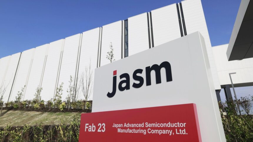
TSMC is considering equipping its upcoming Fab 23 Phase 2 facility in Kumamoto, Japan, with the capability to manufacture chips using its N4 process, a 4nm-class technology, according to a report from Nikkei. The shift would represent a notable enhancement from the originally planned N6 and N7 nodes, aligning the Japanese plant with more advanced production used for high-performance and automotive applications.
The possible upgrade comes amid an unexpected pause in on-site activity. Heavy machinery that had been present during the early construction stages was removed in early December, and suppliers were reportedly told that TSMC would not require new tools for the plant at any point in 2026. This suggests a delay in the installation phase, though TSMC has not offered an official explanation.
Fab 23 phase 1, already in operation, handles mature process technologies ranging from 40nm to 12nm. Phase 2 was initially expected to complement this portfolio by adding 7nm- and 6nm-class production. If the facility adopts N5 and N4 as well, it would substantially expand TSMC’s advanced manufacturing footprint in Japan.
Despite the major differences in design rules and complexity between the N7/N6 and N5/N4 families, the underlying tool sets share a high degree of overlap-TSMC has previously stated that as much as 90% of equipment can be reused between these nodes.
However, migrating to N4 would require additional EUV lithography tools, which are significantly larger and more demanding to integrate into a fab’s layout. TSMC considered introducing N4 capabilities in Kumamoto as early as 2023, indicating that preliminary planning for such an upgrade may already be in place.
Images from the construction site illustrate the abrupt slowdown. After cranes and earth-moving machinery were visible in late October and November, nearly all heavy equipment had been cleared by early December. Vendors were also informed that procurement of new equipment would not move forward next year, reinforcing the expectation that major fit-out work will not occur in 2026.
TSMC declined to comment directly on the reported pause but reiterated its broader timeline. During the company’s most recent earnings call, CEO C.C. Wei confirmed that construction of the second Kumamoto fab had begun and emphasised that future ramp schedules will depend on customer requirements and market demand. Wei also noted that the first Kumamoto fab entered volume production in late 2024 with strong yields.
While the exact reasons for the slowdown remain unclear, the potential upgrade to 4nm-class manufacturing signals TSMC’s continued intention to position Japan as a strategic hub for both advanced and mature semiconductor processes-provided market conditions support the investment.


