
Chinese memory manufacturer ChangXin Memory Technologies, better known as CXMT, has announced a major manufacturing advance with its fifth-generation G5 DRAM platform.
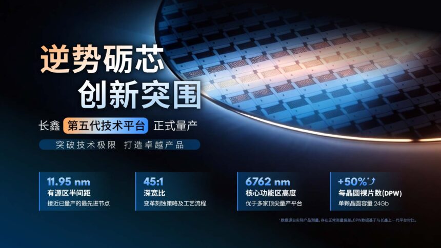
Less than a month after revealing its LPDDR6 memory technology, CXMT says its latest DRAM process has entered mass production, bringing higher memory densities and significantly better wafer productivity. The company claims its new process can produce 50% more DRAM dies per wafer than its previous-generation technology.
CXMT Moves Closer to Leading DRAM Manufacturers
The G5 platform uses an active-area half-pitch of 11.95nm, representing a substantial step forward for CXMT’s DRAM manufacturing technology.
That figure brings the Chinese manufacturer closer to the process capabilities of established DRAM giants such as Samsung, SK Hynix and Micron.
Smaller process dimensions allow CXMT to fit more memory dies per wafer. According to the company, the improvement results in roughly 50% more dies being produced per wafer compared with its previous DRAM generation.
However, there is an important caveat. CXMT has not disclosed detailed manufacturing yield figures for the new process.
That means the company has not demonstrated that it can produce 50% more fully functional DRAM chips per wafer. Higher die density does not automatically translate into an equivalent increase in usable memory if manufacturing yields are lower.
Even so, the reported improvement represents an important step for CXMT.
24Gb LPDDR5X Chips Enter Mass Production
The first confirmed products using the G5 platform are 24Gb LPDDR5X memory chips, which CXMT says have already entered mass production.
Reports from China indicate that the new memory is already being used in Chinese smartphones, giving CXMT an early opportunity to put its latest manufacturing technology into commercial devices.
The higher-density chips could help manufacturers build devices with greater memory capacity without requiring a corresponding increase in the physical space dedicated to DRAM.
More Efficient Production Could Help CXMT Scale
Increasing the number of dies produced per wafer has implications beyond simply making more memory.
If CXMT can maintain competitive yields while increasing wafer productivity, the company could reduce manufacturing costs and improve the economics of its DRAM production. Greater output could also help CXMT expand its presence in a memory market that continues to face supply and pricing pressures.
The company has been working to establish itself as a major global DRAM supplier, competing against manufacturers with decades of experience in advanced memory production.
Its latest G5 process does not necessarily put CXMT on equal footing with Samsung, SK Hynix, or Micron, particularly in the absence of detailed yield data. However, an 11.95nm active-area half-pitch and a claimed 50% increase in dies per wafer indicate that CXMT’s manufacturing capabilities continue to advance.
The company’s move into higher-density LPDDR5X production, followed by its recent LPDDR6 announcement, also suggests that CXMT is rapidly expanding both the capacity and technological range of its memory business.